
PCB DESIGNING COURSE
CERTIFIED
PCB DESIGNER

Duration : 1 Month
Certified Trainer
Dedicated Career Services
Unlimited Interviews
APPLY NOW
POST GRADUATE DIPLOMA IN
INDUSTRIAL IOT & PCB DESIGN
Duration : 3 Months
Certified Trainer
Dedicated Career Services
Unlimited Interviews
APPLY NOW
CERTIFIED
IOT ENGINEER
Duration : 1 Month
Certified Trainer
Dedicated Career Services
Unlimited Interviews
APPLY NOW
CERTIFIED
EMBEDDED ENGINEER
Duration : 1 Month
Certified Trainer
Dedicated Career Services
Unlimited Interviews
APPLY NOW
ADVANCED
EMBEDDED PROFESSIONAL
Duration : 2 Months
Certified Trainer
Dedicated Career Services
Unlimited Interviews
APPLY NOW
POST GRADUATE DIPLOMA IN
EMBEDDED SYSTEMS
Duration : 3 Months
Certified Trainer
Dedicated Career Services
Unlimited Interviews
APPLY NOW
CERTIFIED
EMBEDDED PROFESSIONAL
Duration : 1 Month
Certified Trainer
Dedicated Career Services
Unlimited Interviews
APPLY NOW

PROFESSIONAL
EMBEDDED DEVELOPER
Duration : 3 Months
Certified Trainer
Dedicated Career Services
Unlimited Interviews
APPLY NOW
CERTIFIED
EMBEDDED DESIGN ENGINEER
Duration : 1 Month
Certified Trainer
Dedicated Career Services
Unlimited Interviews
APPLY NOW
PCB DESIGNING TRAINING
Looking for Best PCB Designing Training in Chennai, EGAI is No 1 PCB Designing training institutes in Chennai offering professional training by experts. Call +91-9176-604201, +91-7305-356204.
EGAI is an excellent PCB Designing training center in Chennai with superior integrated infrastructure and newly designed labs for students to practice and pursue training for multiple courses at Chennai. EGAI train many students around the globe every year for the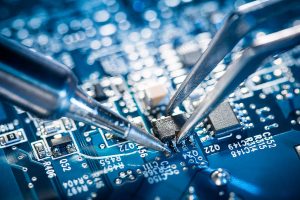 PCB Designing training at an affordable price which is customised as per each candidate’s requirement of modules and content.
PCB Design training course involves “Hands-on experience”, we believe in practice what you preach and therefore each candidate is encouraged to practically conduct each topic that is discussed for better understanding of real-world scenario PCB Design. This practice of comprehensive training allows candidate to gain all the concepts and skills effectively and to later efficiently apply on their field of work.
EGAI is one of the best PCB Design training institute in Chennai with 100% placement assistance. EGAI has well structure modules and training program designed for both students and working professionals separately. At EGAI PCB Design training is conducted during all 5 days, and special weekend classes. Can also be arranged and scheduled. We also provide fast track training programs for students and professionals looking to upgrade themselves instantly.
Why PCB Design Course in Chennai at EGAI?
Chennai is the commercial hub of South India and its home to global manufacturing Electronic companies. Most of the companies looking for trained engineers in the field of PCB design and Embedded. But there is shortage for trained engineers in the PCB Design. To cater the problem, EGAI is offering Best PCB Design Course in Chennai by industry experts designed to fill the vacuum of practical knowledge and industry automation demands. EGAI is best PCB Design Training institute offering PCB Design Course in Chennai with PCB Design theory and practical.
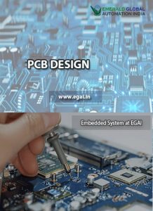
PCB DESIGNING
Breadboards are great for prototyping circuits, but they aren’t so good for actually using the thing you’re building. At some point, you’ll probably want to make a project more permanent. The best way to do that is to put it on a PCB. Process of designing a PCB Design layout and getting it printed by a custom PCB Design manufacturer. The performance of your circuit will depend greatly on how it’s laid out on the PCB Design, so I’ll give you lots of tips on how to optimize your design.
Printed circuit board (PCB) mechanically supports and electrically connects electronic components or components using conductive tracks, pads and other features etched from one or more sheet layers of copper laminated onto and/or between sheet layers of a non-conductive substrate. Components are generally soldered onto the PCB to both electrically connect and mechanically fasten them to it. Printed circuit boards(PCB) are used in all but the simplest electronic products. They are also used in some electrical products, such as passive switch boxes. 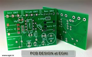 Alternatives to PCBs include wire wrap and point-to-point construction, both once popular but now rarely used. PCBs require additional design effort to lay out the circuit, but manufacturing and assembly can be automated. Specialized CAD software is available to do much of the work of layout. Mass-producing circuits with PCBs is cheaper and faster than with other wiring methods, as components are mounted and wired in one operation. Large numbers of PCBs can be fabricated at the same time, and the layout only has to be done once. PCBs can also be made manually in small quantities, with reduced benefits. PCBs can be single-sided (one copper layer), double-sided (two copper layers on both sides of one substrate layer), or multi-layer (outer and inner layers of copper, alternating with layers of substrate). Multi-layer PCBs allow for much higher component density, because circuit traces on the inner layers would otherwise take up surface space between components. The rise in popularity of multilayer PCBs with more than two, and especially with more than four, copper planes was concurrent with the adoption of surface mount technology. However, multilayer PCBs make repair, analysis, and field modification of circuits much more difficult and usually impractical.
EMBEDDED SYSTEM
Embedded system are an inseparable part of our life. Be it home, office or on the move, we are always surrounded by embedded system. From home appliances like television, washing machine or workplace gadgets like printers, elevators to automobiles or automatic traffic control systems, all work on embedded technologies. Embedded system is an emerging technology, which is attracting a lot of investors from industries like telecom, automobile and other small scale embedded systems. This growth is bringing in a lot of job opportunities in various industries- Research and development is one such sector, which is of great benefit to the Indian market because of the talent it possesses in terms of quality and quantity. We have noticed a vast growth in this sector over the past few years. 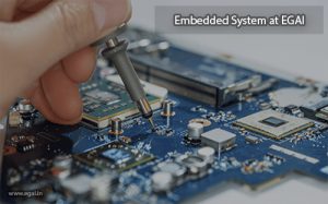 The students are not only attracted towards the handsome salaries that this sector offers, but also the scope for a fresher or a less experienced designer to explore his/her creativity by working on innovative projects. I would state that the freshers, especially from the electronics, computers and operating systems background have the right caliber to start ahead on embedded systems. It is the right time to join this race. In today’s competitive Electronics market scenario, India too holds a market value but as compare to other countries we still feel that a lot needs to be done to prove our potential in electronics (R&D) domain too. Emerald Global Automation India came up with a little initiative to provide our young and budding engineer a platform where they can learn, experiment and express their ability to solve different problems related to our growing economy. So, we offer different courses and arrange different workshop for such engineering students and engineers from time to time. Most of emerging everyday inventions are accompanied with embedded system as a part of its functionality. Experts have predicted that this emergence will never stop in the near future. Thus the bright career opportunities are awaiting in this technology. Students who are studying final year BE/BTECH in ECE, EEE, E&I, CSE, IT should opt IEEE Embedded Systems projects which is show case to recruiters.
- Automation
- Bio-Medical
- Consumer Electronics
- Data Acquisition
- Real Time Operating Systems(RTOs)
- Industrial Electronics
- Control Systems
- Control Area Network (CAN)
- SCADA
- GPS/GSM/GPRS
- Robotics
- Wireless Power Transfer
- Power Line Communication
- Vehicular Technology
- Military Electronics
- Sensor Networks
- Wireless Communication
- Electrical Energy / Power Generation
- Security
- Telematics / Automotive
- Electrical / Motors
- Android / Bluetooth
- Matlab with Hardware
- Embedded Networking
- Sensors / Gesture
- Speech Recognition
SUBSCRIBE OUR YOU TUBE CHANNEL
OUR STUDENTS REVIEW